SEM images of KNbO3 specimens synthesized at 800 °C with varying ...
researchgate.net
Post from YouTube
youtube.com
SEM images of the KNbO3 nanocubes pre…
SANTOSH RATHVA
pinterest.com
FESEM images of (a) KNbO3, (b) 0.5wt% KN…
youtube
SEM images of KNbO 3 (a), ZnO (b), and KNb…
Tanpa Judul
logodownload.org
SEM images of a KNbO3, and b 2.0 mM …
Subscribe Png and bell
SEM images of (a) pristine Nb2O5, (b) N…
YOUTUBE GOLD PLAY BUTTON
SEM images of a KNbO3, and b 2.0 mM-CoO/KNO, c EDS spectrum of ...
YouTube Logo Animation
a Scanning electron microscopic (SEM) image, b …
I love YOUtube 🥰 #funny #couple
m.youtube.com
FE-SEM images of (a) g-C 3 N …
SEM micrographs of hydrothermal produced powde…
Cosas que NO son lo que PARECEN 😱 (Parte 2) #shorts
(PDF) Synthesis of KNbO3 Nanorods by Hydrothermal Met…
You tube logo
(a) SEM image, (b) low magnification TEM image, and (c) HRTEM image of ...
YouTube!
SEM micrograph of the surface of the (K,Na)NbO3 ceramic sintered at ...
SEM images of KNbO3 specimens synthesized at 800 °…
MY FIRST YOUTUBE VIDEO 🤍✨ || Weekly vlog
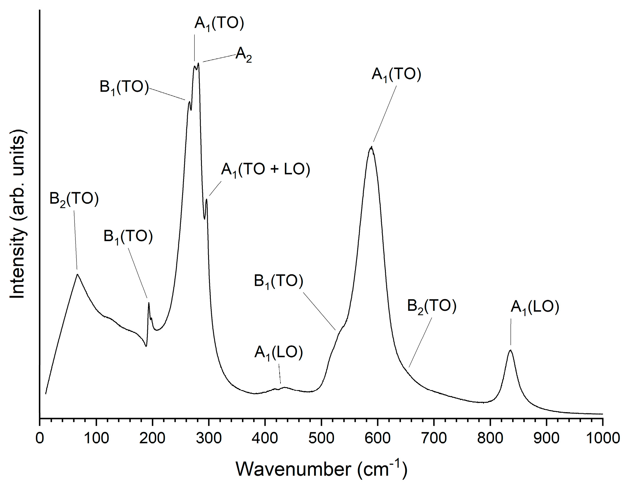
Raman spectrum and decomposed Raman …
AnschuetzGmbH
Controlled-Atmosphere Sintering of KNbO3
mdpi.com
yutube
TEM (transmission electron microscopy) image of KNbO3 NRs synthesized ...
like subscribe
I love YouTube 🥰 @princessameliawu #sofimanassyan #funny #friends
(color online). Radiation from optically trapped single KNbO3 ...
SEM images of the surface of NaNb…
Sintering of Lead-Free Piezoelectric Sodium Potassium Niobate Ceramics
Domain structure in SEM images …
SEM and TEM images of NaNbO3 nanowires (a an…
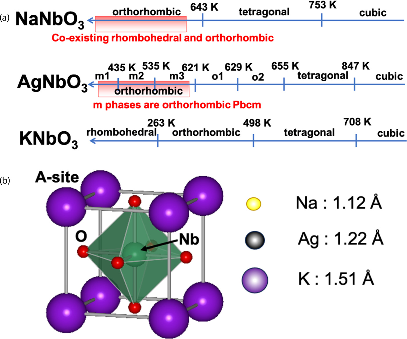
Studies of Optical, Dielectric, Ferroelectric, and Structural Phase ...
SEM images of the KNbO3 nanocubes prepared under diff…
(PDF) Manipulation of charge transfer in vertically aligned epi…
SEM images of KNbO3 specimens synthesiz…
SEM images of (a) pristine Nb2O5, (b) …
Growth of KNbO3 Single Crystals by the Flux Method Using KBO2 …
(a) SEM image, (b) low magnification TEM image, an…
(a) and (b) SEM photographs of a KNbO 3 thin film solvothermally ...
Ferroelectric measurement of M‐KN…
Fig. S5. SEM image of KNbO 3 NWs after the …
(a) SEM image of the KNbO 3 nanoparticles synthesized from …
Ferroelectric measurement of M‐KNbO3 crystals. a) The J–E l…
Low-temperature processing of screen-printed piezoelectric KNb…
europepmc.org
Local and electronic structures of NaNbO3, AgNbO3, and KNbO3 - IOPscience
iopscience.iop.org
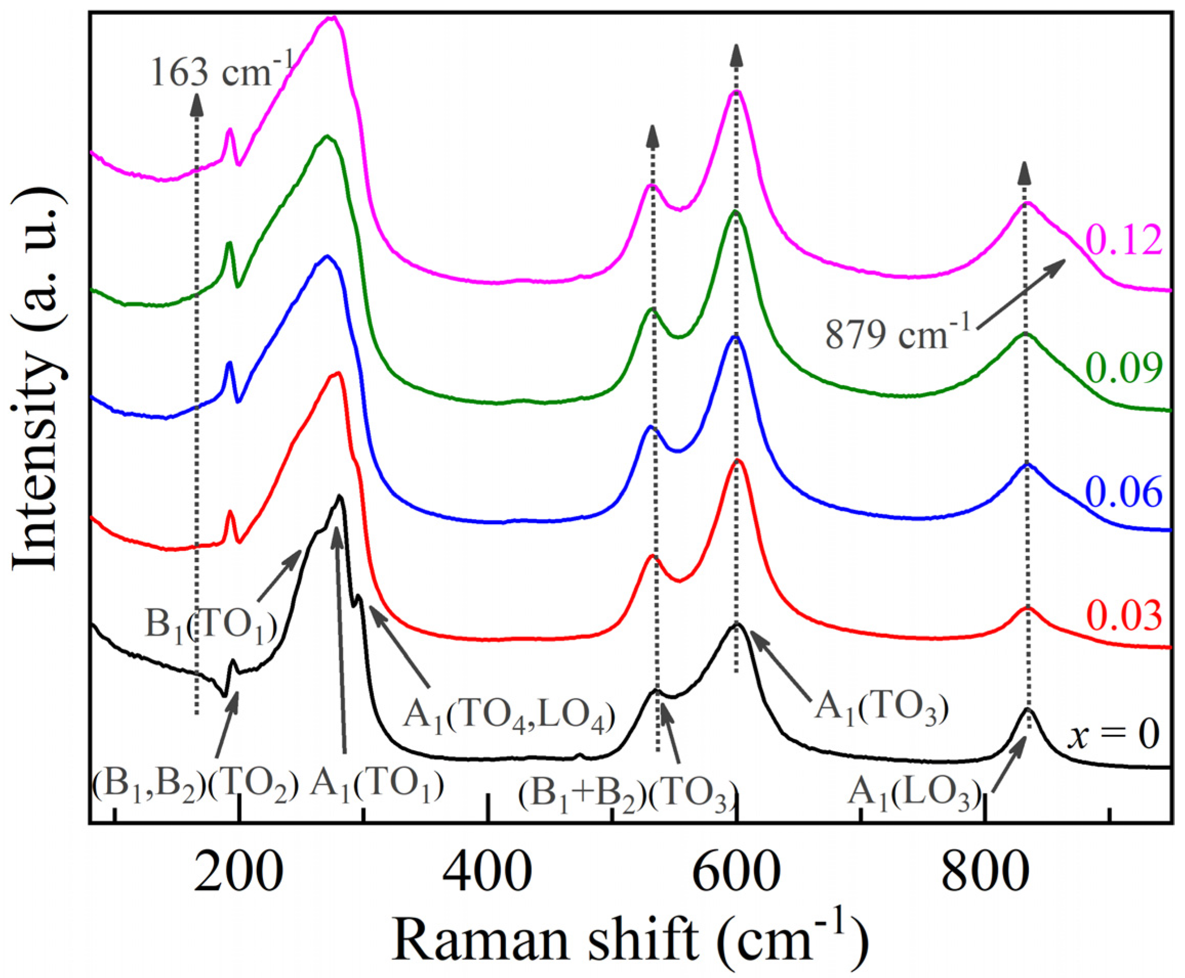
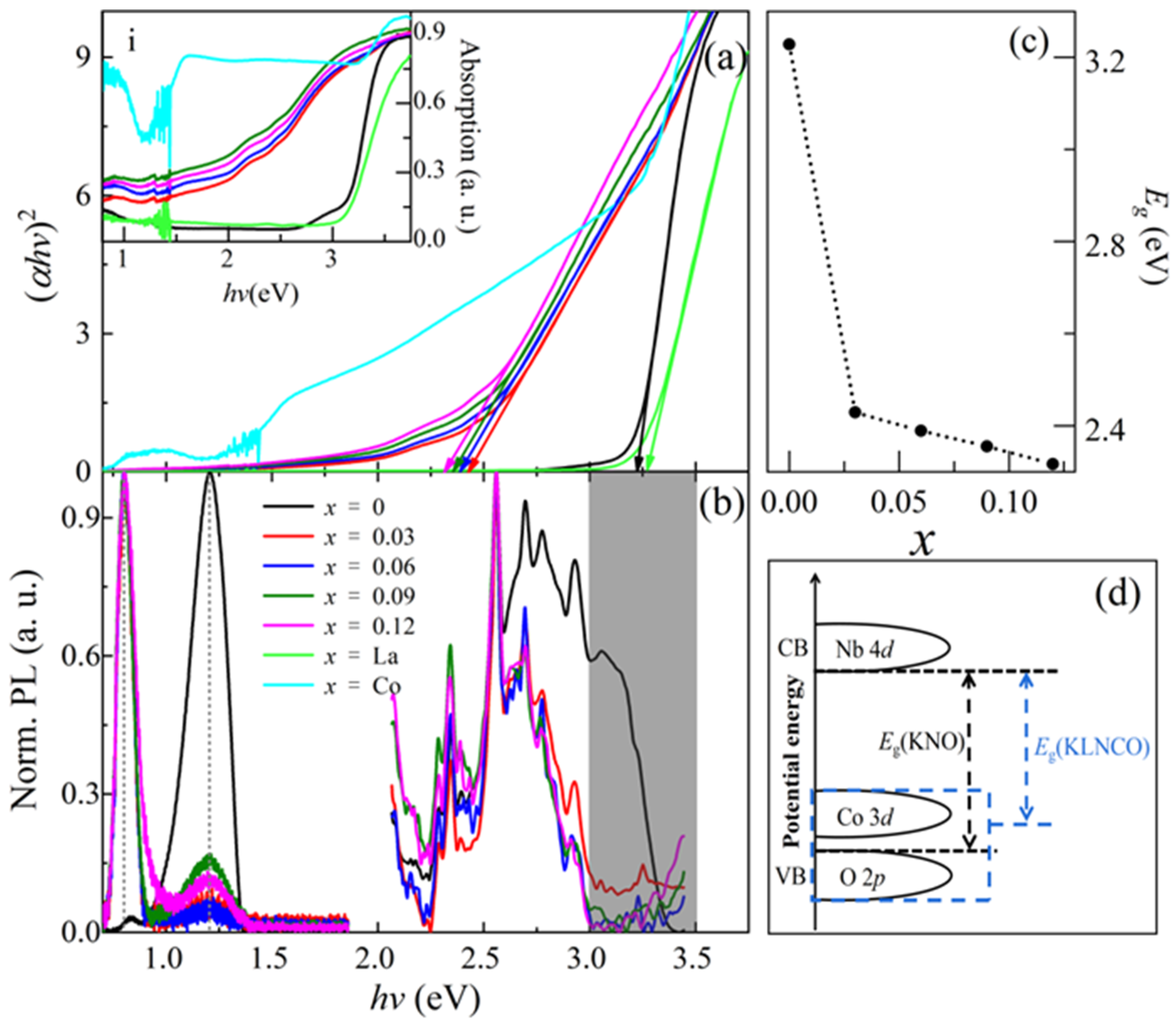
Modulation of Ferroelectric and Optical Properties of La/Co-Doped KNbO3 ...
Representative morphologies of the as-prepared KNbO 3 samples. (A…
TEM (transmission electron microscopy) im…
Modulation of Ferroelectric and Optical Properties of La/Co-Do…
(a) Crystal structure of m-KNbO3. (b) Crystal structure of o-KNbO3. (c ...
SEM micrographs of the KNb 3 O 8 thin fil…
Dislocation‐enhanced piezoelectric catalysis of KNbO3 crystal for water ...
ceramics.onlinelibrary.wiley.com
Perovskite KNbO3 nanost…
Growth of KNbO3 Single Crystals by th…
[보고서]하이브리드 에너지 하베스팅 기술 개발
scienceon.kisti.re.kr
SEM images of synthesized NbC by the calcination of th…
Modulation of Ferroelectric and Optical Properties o…
XPS spectra of pure g-C3N4, …
FT-IR spectra of KNbO3/g-C3N4 composite with variou…
(a) Crystal structure of m-KNbO3. (b) Crystal structure of o-KNbO…
Phase diagram for the KNbO3–NaNbO3 system (after [2, 3]) and dielectric ...
XRD patterns of KNbO3, g-C3N4, and KNbO3/g-C3N4 composite…
Growth of KNbO3 Single Crystals by the Flux Method Using KBO2 as a Flux


![[보고서]하이브리드 에너지 하베스팅 기술 개발](https://nrms.kisti.re.kr/bitextimages/TRKO202100005403/TRKO202100005403_50_image_1.png)


![Phase diagram for the KNbO3–NaNbO3 system (after [2, 3]) and dielectric ...](https://www.researchgate.net/profile/Chang-Ahn/publication/257632129/figure/fig1/AS:297567389798402@1447957002383/a-X-ray-diffraction-patterns-for-the-BNKT15-thin-fi-lm-and-SEM-images-of-the-b_Q320.jpg)